Given the widespread use of semiconductors in various fields today, the semiconductor industry has become a national fundamental and strategic industry. With the rapid development of high-end technologies such as artificial intelligence, the importance of the semiconductor industry has become increasingly prominent.
The Importance of Semiconductors
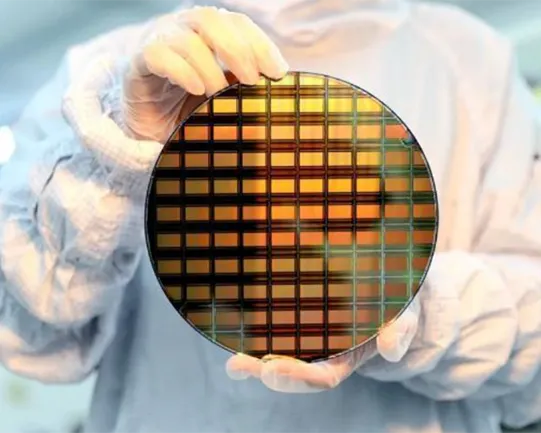
Chip (integrated circuit) manufacturing technology is currently the pinnacle of global micro-processing technology and represents the commanding heights for high-tech competition among countries worldwide, significantly reflecting a nation’s high-tech strength. As the key electronic materials used to make chips, semiconductor materials are the cornerstone of the entire semiconductor industry.
Chips, as core electronic components, are widely used in numerous fields such as computers, communications, industrial control, and healthcare, and their importance is self-evident. Within the semiconductor industry, particularly in the research, development, manufacturing, and testing stages of chips, the requirements for product quality and reliability are extremely high.
Traditional inspection methods may have certain limitations and struggle to meet the detection needs of increasingly sophisticated semiconductor devices.
Application of Thermal Imaging Inspection for Semiconductor Industry
Infrared thermal imaging technology, known for its non-contact, high accuracy, and visual capabilities, has become an essential tool in semiconductor testing. By capturing real-time temperature distribution and thermal radiation signals, this technology effectively overcomes the shortcomings of traditional inspection methods, helping the industry address process challenges and improve both yield and product reliability.
Below are its core application scenarios and typical use cases:
1. WLP Testing and Packaging Defect Location
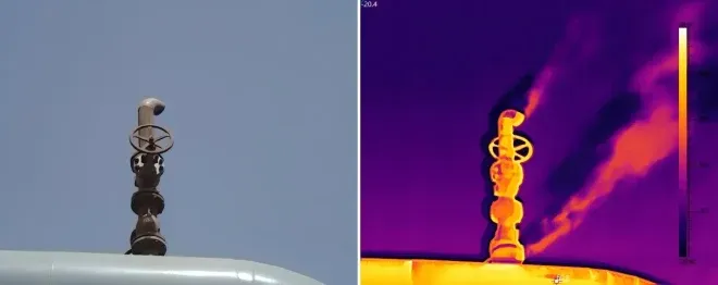
Infrared thermal imaging can penetrate silicon-based materials, allowing for non-destructive testing of both surface and internal structures of wafers. For example, during the wafer grinding process, infrared radiation from both the front and back of the silicon substrate enables precise measurement of grinding depth and optimization of process parameters. In flip-chip packaging, this technology can detect defects like solder leakage and copper wire corrosion by penetrating the silicon substrate, thus avoiding the physical damage that traditional inspection methods might inflict on components.
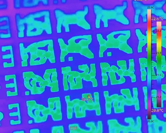
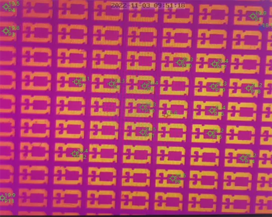
2. LED Chip Temperature Monitoring
The LED chip is a solid-state semiconductor device. Its core is a semiconductor chip. One end of the chip is negative and attached to a bracket, while the other end is connected to the positive electrode of the power supply, enabling the entire package by epoxy resin. During the production process of LED chips, there will be insufficient curing of silver glue, contamination of brackets or chip electrodes, resulting in large contact resistance or unstable contact resistance, and other adverse phenomena like temperature rise. Compared with traditional monitoring solutions, thermal cameras provide a more obvious and direct monitoring result, displaying more objectively defect locations of LED chips.
They offer a significant advantage by providing a non-contact and real-time visual representation of the LED chip’s temperature distribution. This allows for the immediate identification of localized hotspots indicative of defects like insufficient silver glue curing or contamination causing increased electrical resistance. The resulting thermal image objectively pinpoints the location of these issues, enabling faster diagnosis and more targeted corrective actions compared to indirect electrical measurements or subjective visual assessments.
3. Precise Location of Microscopic Defects and Hotspots in Semiconductor Devices
Defects such as cracks and micro-short circuits in semiconductor devices often lead to localized temperature anomalies. By detecting variations in thermal distribution, thermal cameras can quickly and precisely pinpoint hotspot areas on the chip. Infrared thermal images allow for the rapid and accurate location of these high-temperature points within the device, eliminating the need for detailed circuit design analysis. This key characteristic has fueled the widespread adoption and ongoing research of infrared thermal imaging in semiconductor inspection.

4. Heat Dissipation Design and Thermal Management Validation
During the chip design process, thermal cameras, utilizing non-contact infrared detection, enable real-time monitoring of temperature rise in circuit boards or packaging components, helping engineers optimize heat dissipation structures. These cameras capture detailed thermal maps, revealing even subtle temperature variations across the surface of the device. For instance, by analyzing the temperature distribution of power devices under dynamic loads, engineers can observe the precise location and intensity of heat generation. This allows them to effectively refine heat dissipation solutions, such as the placement and design of heat sinks, to reduce the risk of thermal runaway.
Sophisticated software accompanying these thermal cameras often provides tools for quantitative analysis, allowing engineers to measure peak temperatures and temperature gradients and track thermal behavior over time, further aiding in the validation and optimization of thermal management designs.

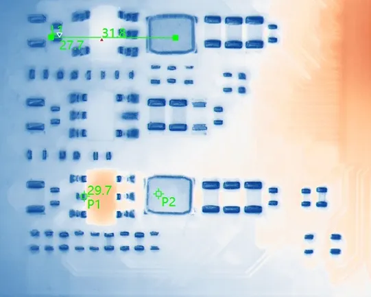
5. Circuit Board Environmental Test
During the design and test of the circuit board, researchers need to monitor the temperature of the electronic components in the circuit board to figure out the temperature load of each component. During the test, it is necessary to simulate the actual working environment of the circuit board and observe the temperature state of electronic components from power-on to stabilization. As electronic components in the circuit board are highly exquisite, traditional contact temperature measurement equipment is complicated to work with and cannot meet the testing requirements of scientific researchers.
In contrast, thermal cameras offer a highly effective solution for this application. Their non-contact nature allows researchers to safely and easily monitor the temperature of even the smallest and most delicate electronic components without any physical interference. Providing real-time thermal imaging, these cameras enable the observation of temperature changes across the entire circuit board as it powers up and reaches a stable state. Researchers can simultaneously monitor the temperature of multiple components, gaining a comprehensive understanding of the thermal load distribution. Furthermore, the data captured by thermal cameras can be easily recorded and analyzed, providing valuable insights into the thermal behavior of the circuit board and its components under various operating conditions, ultimately facilitating optimized design and reliable performance.

6. Dynamic Test
Infrared thermal imaging is essential for dynamic performance testing of semiconductors under extreme conditions and high currents. With wide temperature ranges and high sensitivity, thermal cameras record real-time temperature rise curves during tests like varying current applications by a probe station. This prevents overheating errors and allows engineers to observe the device’s thermal response to dynamic loads. Advanced software enables detailed analysis of temperature gradients and heat dissipation, revealing potential failure mechanisms and facilitating correlation with electrical performance data for optimized design and reliability.
7. Semiconductor Equipment Temperature Monitoring
Continuous thermal monitoring using fixed or handheld thermal cameras is crucial for high-value semiconductor equipment like lithography machines and ion implanters to detect abnormal temperature rise in critical components such as motors, bearings, power supplies, and cooling systems, enabling early warnings and preventing costly downtime. This proactive approach supports predictive maintenance, reducing maintenance expenses and extending equipment lifespan.
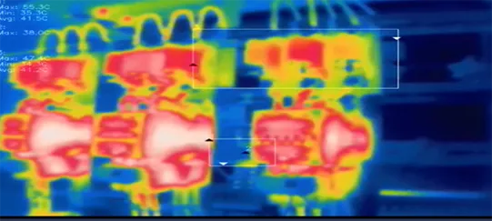
8. Power Distribution Cabinet Temperature Monitoring
The power distribution cabinet is arranged with equipment and devices densely, resulting in a complicated electromagnetic environment. The local resistance of the contact parts of power distribution equipment, cables, bus connectors, and electrical switch contacts may increase and heat up due to poor contact, material aging, wear, and other reasons; building in fire hazards; traditional monitoring equipment features complex equipment installation, unclear target temperature distribution, detection omission, difficult maintenance, slow response, heat conduction time, and poor timeliness.
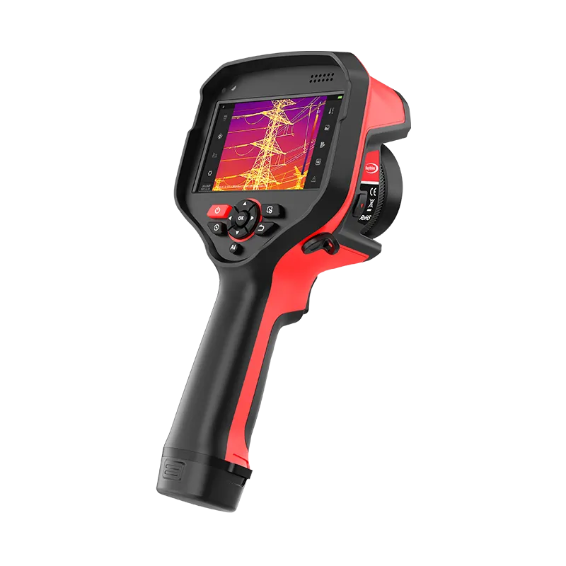
Because of the complex equipment and narrow space in HV switchgear, a light and convenient pocket camera TN220 is designed to realize real-time monitoring, defect diagnosis, alarm output, and other functions of equipment in the cabinet. This is a reliable infrared equipment solution for safe and stable operation and online video patrol inspection of equipment in the distribution cabinet. In addition, different software applications are configured according to different scenario requirements, i.e., lightweight real-time monitoring client and converged media cloud platform.
Technical Advantages of Infrared Thermal Cameras
- Non-contact testing: It is able to avoid physical damage to semiconductor materials, especially suitable for precision testing of micron-sized chips.
- Real-time and wide-area coverage: It is able to quickly obtain large-area temperature distribution data and support dynamic process monitoring.
- Accurate defect positioning: It is able to identify invisible defects such as cracks and microcracks through abnormal heat distribution to reduce manual misjudgment.
As the complexity and integration of semiconductor devices continue to grow, infrared thermal imaging technology will become increasingly integral to the smart manufacturing ecosystem, acting as a key driver for ensuring chip reliability and advancing process innovation.
Application Cases of Raythink Infrared Thermal Camera
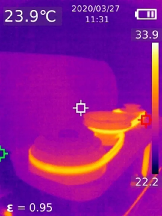
1. Temperature Measurement in LED Chip Manufacturing
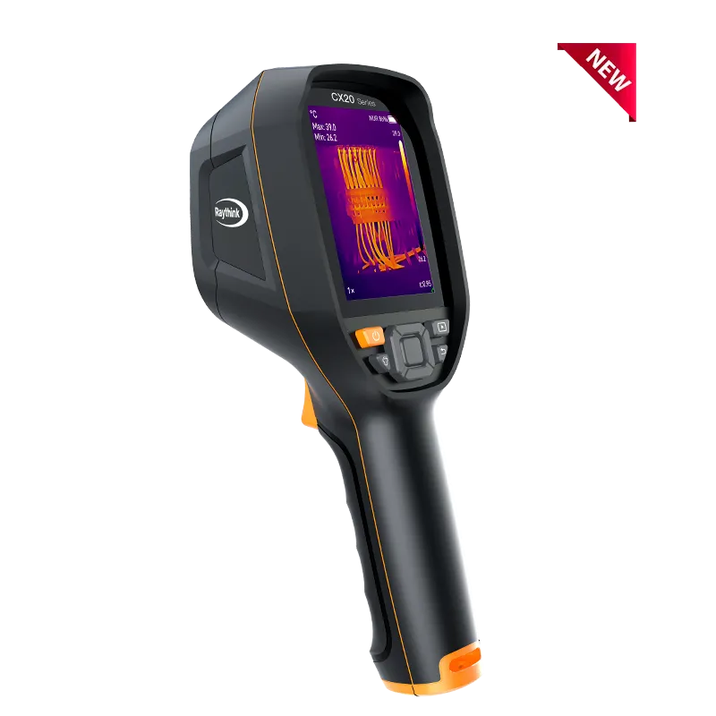
During the production process of LED chips, there will be insufficient curing of silver glue, contamination of brackets or chip electrodes, resulting in large contact resistance or unstable contact resistance, and other adverse phenomena like temperature rise. Compared with traditional monitoring solutions, thermal cameras provide a more obvious and direct monitoring result, displaying more objectively defect locations of LED chips. In this project, our thermal camera TN460 is deployed above the LED chip to monitor the temperature in the core area in real time. With our professional temperature analysis software “TI studio”, it can clearly identify chip defects.


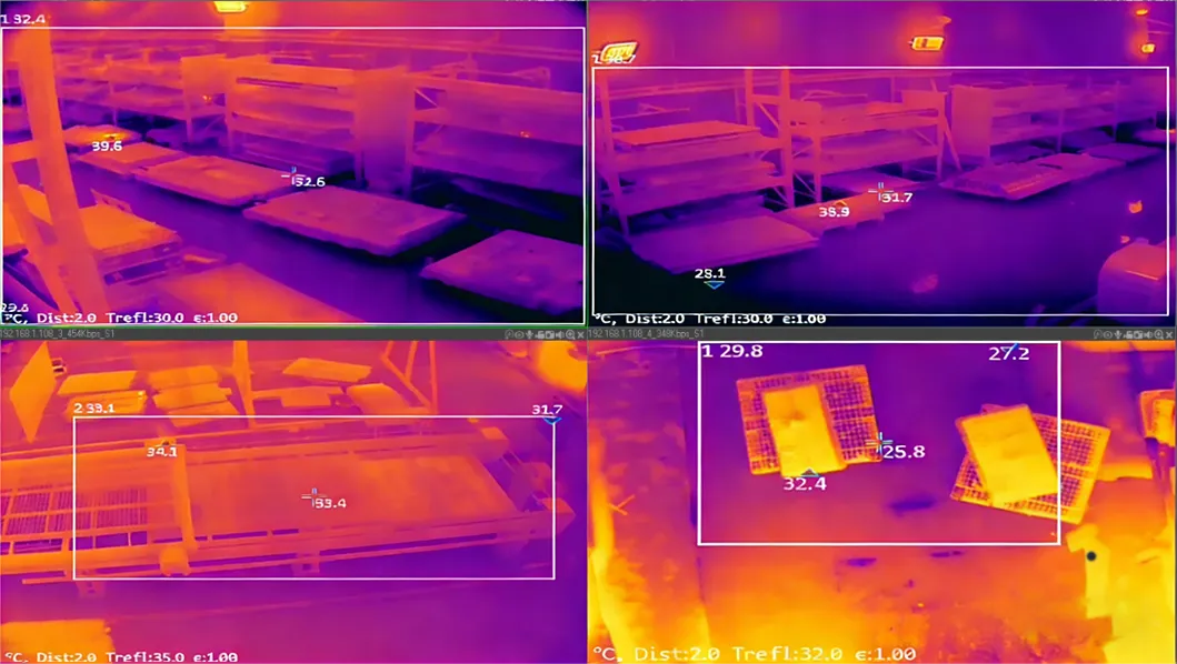
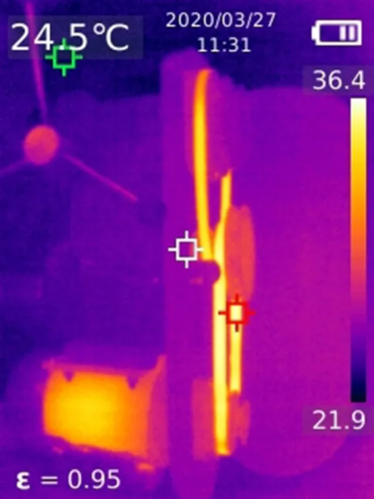
2. Temperature Measurement in Circuit Board Manufacturing
As electronic components in the circuit board are highly exquisite, traditional contact temperature measurement equipment is complicated to work with and cannot meet the testing requirements of scientific researchers. In this project, the online electrically tuned temperature measurement thermal camera AT61 is installed above the circuit board for imaging and temperature measurement without contact. In addition, to simulate the actual working environment of circuit boards, the thermal camera and the circuit board are placed in a thermostat for observation at the same time. Even when the maximum temperature of the thermostat reaches 60 °C, our camera is still able to accurately measure the temperature.


.webp)

.webp)